Serial to I2C Conversion
Serial to I2C Converters have a unique benefit in the electronics industry. When properly structured, they can open a computer up to unlimited expansion potential. In this article, we will discuss how to use NCD I2C conversion devices, which will allow you to connect virtually any kind of device to a computer and take control in a matter of minutes. We have prepared several samples and software tools to help get you started, so you can hit the ground running with a converter that was designed for compatibility and more expandability than you might realize.
NCD has been manufacturing Serial to I2C Converters for some time now, but the most recent firmware improvements are easier to use and can save you a lot of time. It’s now possible to talk to any I2C device with only a few commands. Whether you are working with a PC or embedded micro, this guide will demonstrate the commands needed to read any kind of sensor or control any kind of I2C device.
This command reference guide will help get you started using AnyI2C hardware and software using our latest V6 hardware communications protocols. If you’ve been following us on ncd.io, you will notice that all devices are now shipping with AnyI2C V3 firmware. Here we will explain the improvements with detailed samples to help get you started quickly.
Hint: NCD’s new V6 Serial to I2C Conversion processor understand TWO protocols. NCD API as well as 900HP-S3B Wireless. In future tutorials, we will show you how the same processor will allow for Wireless I2C Communications. This will allow you to make ANY NCD I2C Device into a Wireless I2C Device using the same serial to I2C converter CPU, which automatically detects and adapts to BOTH protocols!


V3 Feature Overview
- I2C Communications is now hardware, not software, Improving Reliability and Compatibility
- I2C Communications speed has increased from 38KHz to 100KHz default
- I2C Communications Speeds of 200, 300, and 400KHz are now possible
- I2C Clock Stretching Functions have been Improved
- A simplified I2C Write command has been added
- A simplified I2C Read command has been added
- AnyI2C Firmware V3 now Supports Wireless I2C Communications
- Automatic Protocol Detection of Wireless vs NCD Protocols
- Simply Wrap a Wireless API Frame Around the NCD API Frame
V4 Feature Overview
Orders Shipping 6/27/2019 through 7/30/2019 Include Updated firmware to Issue a Stop Command Regardless of Error or No-Error on the I2C Bus. This version also includes all Version 3 Changes.
V5 Feature Overview
Orders Shipping 7/31/2019 through 8/1/2019 and Later Include Updated firmware to Make the Stop Command in Version 4 Optional. As the CPU is currently very full, code has been optimized in this version to reduce memory usage, Clearing the way for a Version 6.
To Use Version 4 Changes, Please Download Base Station at https://ncd.io/start and click on “I2C Converter Device Configuration” and Un-check the “Reserved” Check Box, and be Sure to “Save Settings”. Later Versions of Base Station will Indicate this option as “Smart I2C Stop”.
This change was Necessary as Version 4 Prevented Proper Operation of I2C Bus Scan Features in AnyI2C Software.
V6 Feature Overview
Orders Shipping 8/2/2019 and Later now include Version 6, which is nearly our final release version of firmware for this device. Version 6 includes many improvements over version 5. Like Version 5, this device is configured using Alpha Station 1.0.0.5 or later. Alpha Station 1.0.0.6 or later is required to take full advantage of device settings. The following features were added to Version 6 Firmware.
- Now Supports I2C Bus Scan
- Now Supports I2C Bus Speed Selection Stored in EEPROM
- Now Supports Bootup of I2C Bus Speed of 38, 100, 200, 300, and 400 KHz
- Added a I2C Write + Read Command for Faster Communications with a Single Transaction
- Added a Soft Reboot Command
- Added a Hard Reboot Command
- Added a Manual I2C Stop Command
- Removed Support for Base Station Software (Not Enough Room in CPU)
NCD API
BEFORE sending anything to NCD Serial to I2C Converters, the NCD API protocol must be discussed. The NCD API serves to protect all communication commands by wrapping them with a standardized header and checksum. NCD devices will ignore any data that does not conform to the NCD API package standard. As you can see, the NCD API format is essential.
Transmitting Data
Before we dig too deep, it’s important to know the default communications baud rate is always 115.2K Baud. Now let’s dig into our first I2C communications command. The following command, 0xFE 0x21 is a simple test for 2-way communications between the device and the controller. They are identified as Payload bytes in the packet structure shown below. Since there are two Payload bytes, Byte 2 of the NCD API Frame must contain 0x02. This number will always scale with the number of payload bytes in the API frame.
| Byte 1 | 0xAA | NCD API Header Byte | |
| Byte 2 | 0x02 | NCD API Byte Count | |
| Byte 3 | 0xFE | Payload Byte 1 | Command Header |
| Byte 4 | 0x21 | Payload Byte 2 | Test 2-Way Communications |
| Byte 5 | 0xCB | NCD API Checksum | 0xAA + 0x02 + 0xFE + 0x21 = 0xCB |
Calculating the Checksum is relatively easy. The checksum value is always truncated to the lower 8 bits and is calculated by adding Bytes 1 through 4 together. There are a couple of easy ways to truncate the value to the lower 8 bits. The easiest way is to define a variable that is only a byte in size. Most programming languages will automatically truncate if the checksum is defined as a byte rather than a word or an integer.
Other programming languages may require you to accumulate the value as a integer or a word. In this case, the lower 8 bits must be extracted using the mathematical AND function. In the above example, 0xAA + 0x02 + 0xFE + 0x21 = 0x01CB.
To extract the lower 8 bits, simply use the Bitwise AND function: 0x01CB AND 0xFF = 0xCB
Some programming languages also allow you to use the << function to shift bits to the left.
Receiving Data
In the previous section of this guide, we demonstrated how to send data to the Serial to I2C Converter at a baud rate of 115.2K Baud. If you actually sent the data to a NCD controller, you should receive the following response packet (or something very similar):
| Byte 1 | 0xAA | NCD API Header Byte | |
| Byte 2 | 0x01 | NCD API Byte Count | |
| Byte 3 | 0x55 | Payload Byte 1 | Response Byte |
| Byte 4 | 0x00 | NCD API Checksum | 0xAA + 0x01 + 0x55 = 0x00 |
The response packet above also includes a checksum for the 4th byte. This checksum is calculated in the exact same way as the transmission packet.
Communicating to I2C Devices
Communicating to I2C devices over a serial connection presents some unique challenges. We have hidden these challenges from the user to help simplify communications. We will not go into the full depth of I2C communications here, as the topic is too far outside the scope of this guide. Instead, we will focus on the two essential elements of communicating to I2C devices: Transmitting and Receiving. All I2C devices have a start address. This start address will be referenced in all transmit and receive operations. It’s also helpful to understand that it is often necessary to send data to a I2C device then read data from a I2C device. For instance, you will often be required to write to the I2C device to move the pointer to a specific register. Using a second operation, you will read data from the register. It is normal to write and then read from a I2C device using two transactions.
NCD Serial to I2C Converters use hardware interrupts for USART communications as well as hardware I2C features of the AnyI2C processor. Hardware USARTS and I2C ports make for more stable communications in the long run. Some I2C chips may be slow to provide a response. In some cases, it may be necessary to send several communication queries to a given device to check flags and read data once the device is ready. We will try to provide numerous samples for talking to many kinds of I2C devices.
Serial Communications
As we progress through the samples shown below, it will be necessary for you to have some mechanism of communications to the AnyI2C processor via the USART. There are many ways to do this, including Ethernet, Wireless, USB, or RS-232. In some cases, the AnyI2C processor is installed on a hat or shield, ready to work with another microprocessor. This guide will focus on communications through a virtual COM port USB interface operating at 115.2K Baud, 8 Data Bits, 1 Stop Bit, No Parity. We will be using Comm Operator as we advance through the samples. Comm Operator is our preferred tool for testing ALL controllers we manufacture.
Comm Operator is available from SerialPortTool.com. DO NOT USE PuTTY or HyperTerminal to communicate to this device as this device is expecting Bytes of data rather than ASCII Text. While it may be possible to configure these applications for Bytes of Data, Comm Operator will automatically calculate the necessary checksums when set to “NCD Board” in the configuration pull-down menus.
I2C Write: Transmitting I2C Data
Transmitting data to I2C devices will require 3 essential ingredients: Knowledge of the I2C Device (including the start address), Knowledge of the I2C Write Command and it’s structure, and Wrapping the I2C Command into a NCD API Frame (discussed earlier). Once you have an understanding of these 3 essential components, writing I2C data is very straightforward.
The command structure for an I2C Write Operation is as follows:
0xBE, <I2C Start Address>, <Data Byte 1>, <Data Byte 2>, <Data Byte 3>, etc.
Data bytes are optional for some I2C chips, as it all depends on the memory organization of each individual I2C device. The data byte buffer is 25 bytes for small 8-pin AnyI2C processors and 100 bytes for larger AnyI2C processors.
Like all commands, I2C Write commands must be wrapped with a NCD API Frame. Take a look at the sample below.
| Byte 1 | 0xAA | NCD API Header Byte | |
| Byte 2 | 0x04 | NCD API Byte Count | |
| Byte 3 | 0xBE | NCD API Payload Byte 1 | I2C Write Command |
| Byte 4 | 0x41 | NCD API Payload Byte 2 | I2C Start Address |
| Byte 5 | 0x03 | NCD API Payload Byte 3 | I2C Data Byte |
| Byte 6 | 0x00 | NCD API Payload Byte 4 | I2C Data Byte |
| Byte 7 | 0xB0 | NCD API Checksum | 0xAA + 0x04 + 0xBE + 0x41 +0x03 + 0x00 = 0xB0 |
The above command works with the PCA9536 programmable GPIO chip. If you happen to have this chip connected, you will receive the following response:
| Byte 1 | 0xAA | NCD API Header Byte | |
| Byte 2 | 0x01 | NCD API Byte Count | |
| Byte 3 | 0x55 | Payload Byte 1 | Command was Successful |
| Byte 4 | 0x00 | NCD API Checksum | 0xAA + 0x01 + 0x55 = 0x00 |
I2C Read: Receiving I2C Data
Receiving data from I2C devices is very similar to transmitting. This operation is relatively easy, since it only requires a I2C Start Address and the total number of bytes to read from the I2C device. Please note that a read operation typically follows a write operation.
The command structure for an I2C Read Operation is as follows:
0xBF, <I2C Start Address>, <Number of Bytes to Read>
Read up to 25 bytes for small 8-pin AnyI2C processors and 100 bytes for larger AnyI2C processors.
This sample will be a little more complicated, as we need to do a little bit of setup before we can read from the PC9536 chip. We will start with configuring the PCA9536 for input mode. This only needs to be done one time to initialize the inputs for reading inputs. Next, we will move the address pointer to location 0. This memory address will reflect the status of the digital inputs. Finally, we will perform a read operation and examine the result.
Step 1: Configure PCA9536 for Inputs
The PCA9536 include 4 programmable GPIO pins. To read inputs, the following commands must be sent to the PCA9536 to configure the GPIO pins into Input mode. Without this step, the inputs will never appear to change state.
| Byte 1 | 0xAA | NCD API Header Byte | |
| Byte 2 | 0x04 | NCD API Byte Count | |
| Byte 3 | 0xBE | NCD API Payload Byte 1 | I2C WriteCommand |
| Byte 4 | 0x41 | NCD API Payload Byte 2 | I2C Start Address PCA9536 |
| Byte 5 | 0x03 | NCD API Payload Byte 3 | PCA9536 Memory Location 0x03 |
| Byte 6 | 0xFF | NCD API Payload Byte 3 | PCA9536 Input Mode (0x00 = Out) |
| Byte 7 | 0xAE | NCD API Checksum | 0xAA + 0x04 + 0xBE + 0x41 + 0x03 + 0xFF = 0xAE |
The controller will respond with the following bytes:
| Byte 1 | 0xAA | NCD API Header Byte | |
| Byte 2 | 0x01 | NCD API Byte Count | |
| Byte 3 | 0x55 | Payload Byte 1 | Command was Successful |
| Byte 4 | 0x00 | NCD API Checksum | 0xAA + 0x01 + 0x55 = 0x00 |
Step 2: Move PCA9536 Address Pointer
The PCA9536 includes a small memory register used for various settings. Location 0 may be used to read the inputs of all GPIO pins. Before every read operation, the address pointer must be relocated to address location 0.
| Byte 1 | 0xAA | NCD API Header Byte | |
| Byte 2 | 0x03 | NCD API Byte Count | |
| Byte 3 | 0xBE | NCD API Payload Byte 1 | I2C Write Command |
| Byte 4 | 0x41 | NCD API Payload Byte 2 | I2C Start Address PCA9536 |
| Byte 5 | 0x00 | NCD API Payload Byte 3 | Move Pointer to Location 0 |
| Byte 6 | 0xAC | NCD API Checksum | 0xAA + 0x03 + 0xBE + 0x41 + 0x00 = 0xB0 |
The controller will respond with the following bytes:
| Byte 1 | 0xAA | NCD API Header Byte | |
| Byte 2 | 0x01 | NCD API Byte Count | |
| Byte 3 | 0x55 | Payload Byte 1 | Command was Successful |
| Byte 4 | 0x00 | NCD API Checksum | 0xAA + 0x01 + 0x55 = 0x00 |
Step 3: Read PCA9536 Inputs
The PCA9536 includes a small memory register used for various settings. Location 0 may be used to read the inputs of all GPIO pins. Before every read operation, the address pointer must be relocated to address location 0.
| Byte 1 | 0xAA | NCD API Header Byte | |
| Byte 2 | 0x03 | NCD API Byte Count | |
| Byte 3 | 0xBF | NCD API Payload Byte 1 | I2C Read Command |
| Byte 4 | 0x41 | NCD API Payload Byte 2 | I2C Start Address |
| Byte 5 | 0x01 | NCD API Payload Byte 3 | Read 1 Byte from I2C Chip |
| Byte 6 | 0xAE | NCD API Checksum | 0xAA + 0x03 + 0xBF + 0x41 + 0x01 = 0xAE |
The above command works with the PCA9536 programmable GPIO chip. If you happen to have this chip connected, you will receive the following response:
| Byte 1 | 0xAA | NCD API Header Byte | |
| Byte 2 | 0x01 | NCD API Byte Count | |
| Byte 3 | 0x36 | NCD API Payload Byte 1 | Byte Returned from I2C Chip |
| Byte 4 | 0xE1 | NCD API Checksum | 0xAA + 0x01 + 0x36 = 0xE1 |
To read inputs continuously, repeat steps 2 and 3 above.
I2C Write Read Command
This Command Requires Version 6 Firmware or Later.
In an effort to reduce serial communications, the I2C Write Read Command was introduced. This command sends data to a I2C Chip, waits a user defined period of time, and then reads data from the I2C Chip. The command Structure is as follows:
0xC0, <I2C Start Address>, <Number of Bytes to Read>, <Delay Between Write and Read>, <Write Data Byte 1>, <Write Data Byte 2>, <Write Data Byte 3>, etc.
This command begins with a header of 0xC0, which tell the Serial to I2C Converter to initiate a Write Read transaction with a I2C device.
The <I2C Start Address> is the address of the I2C chip you would like to communicate to.
The <Number of Bytes to Read> indicates how many bytes you would like to read from the I2C device, typical values are 1 to 4, but larger values are possible to to 16 bytes.
The <Delay Between Bytes> is a value from 0 to 255 which indicates the time between a write and a read transaction. A value of 0 indicates no delay. Longer values may be needed for some I2C chips such as Analog to Digital Converters. If you experience communication errors with this command, try lengthening the time between write and read operations, this can usually resolve communication errors.
Lastly, the <Write Data Byte> is a list of bytes, up to 16, which can be sent to the I2C device.
Once all of these parameters are included and wrapped in a NCD API Structure, the converter will issue a Write Operation, Wait, and then Read the Number of Bytes indicated.
The following sample will communicate to a MCP3428 and reads 2 bytes of data back from the I2C chip:
| Byte 1 | 0xAA | NCD API Header Byte | |
| Byte 2 | 0x05 | NCD API Byte Count | |
| Byte 3 | 0xC0 | NCD API Payload Byte 1 | I2C Write Read Command |
| Byte 4 | 0x68 | NCD API Payload Byte 2 | I2C Start Address |
| Byte 5 | 0x02 | NCD API Payload Byte 3 | Number of Bytes to Read from the I2C Device |
| Byte 6 | 0x16 | NCD API Payload Byte 4 | Delay Between I2C Write Read Command |
| Byte 7 | 0x10 | NCD API Payload Byte 5 | Write a Data Byte |
| Byte 8 | 0xFF | NCD API Checksum | 0xAA + 0x05 + 0xC0 + 0x68 +0x02 + 0x16 + 0x10 = 0xFF |
The MCP3428 will Respond with 5 Bytes of Data:
| Byte 1 | 0xAA | NCD API Header Byte | |
| Byte 2 | 0x02 | NCD API Byte Count | |
| Byte 3 | 0x00 | NCD API Payload Byte 1 | Byte 1 Returned from I2C Chip |
| Byte 4 | 0x01 | NCD API Payload Byte 2 | Byte 2 Returned from I2C Chip |
| Byte 5 | 0xAD | NCD API Checksum | 0xAA + 0x01 + 0x36 = 0xE1 |
I2C Bus Scan Command
This Command Requires Version 6 Firmware or Later.
The I2C Bus Scan Command will scan the I2C Bus and Return a list of Discovered I2C Start Addresses currently connected. This command must be Wrapped in NCD API Structure like all other commands and will return data in API structure.
0xC1, 0x00 Issues the I2C Bus Scan Command when Wrapped in the NCD API Structure
| Byte 1 | 0xAA | NCD API Header Byte | |
| Byte 2 | 0x02 | NCD API Byte Count | |
| Byte 3 | 0xC1 | NCD API Payload Byte 1 | I2C Bus Scan Command |
| Byte 4 | 0x00 | NCD API Payload Byte 2 | Required Parameter for this This Command is 0 |
| Byte 5 | 0x6D | NCD API Checksum |
This Serial to I2C Converter will return a list of I2C Devices, an example can be seen below:
| Byte 1 | 0xAA | NCD API Header Byte | |
| Byte 2 | 0x05 | NCD API Byte Count | |
| Byte 3 | 0x00 | NCD API Payload Byte 1 | 0x00 Display Detected |
| Byte 4 | 0x20 | NCD API Payload Byte 2 | 0x020 MCP230xx Relay Controller Detected |
| Byte 5 | 0x21 | NCD API Payload Byte 3 | 0x021 MCP230xx Relay Controller Detected |
| Byte 6 | 0x68 | NCD API Payload Byte 4 | 0x68 MXP3428 ADC Converter Detected |
| Byte 7 | 0x77 | NCD API Payload Byte 5 | 0x77 I2C Multiplexer Detecte |
| Byte 8 | 0xCF | NCD API Checksum | 0xAA + 0x04 + 0x00 + 0x20 + 0x21 + 0x77 + 0x66 = Checksum |
I2C Stop Command
This Command Requires Version 6 Firmware or Later.
The I2C Stop Command may be issued at any time to return the I2C Bus to the default state. This command may prove useful in the event an error occurs communicating with a I2C device.
0xAA 0x03 0xFE 0x21 0xBB 0x87 I2C Stop Command Shown inside a NCD API Wrapper. Actual Command is 0xFE 0x21 0xBB
This command will return 0x55 inside a NCD API Wrapper:
0xAA 0x01 0x55 0x00
I2C Converter Reboot Command
This Command Requires Version 6 Firmware or Later.
There are two commands that may be issued to the Serial to I2C Converter for the purposes of rebooting the firmware. We have never seen a need for these commands, but we included them just in case. Soft reboot simply restarts the firmware from the beginning. By contrast, Hard reboot crashes the Serial to I2C Converter firmware, forcing the internal watchdog timer to reboot the CPU.
0xAA 0x03 0xFE 0x21 0xBC 0x88 Soft Reboot Command Shown inside a NCD API Wrapper. Actual Command is 0xFE 0x21 0xBC
0xAA 0x03 0xFE 0x21 0xBD 0x89 Hard Reboot Command Shown inside a NCD API Wrapper. Actual Command is 0xFE 0x21 0xBD
I2C Error Codes
Communicating to I2C devices is not always a successful operation. There are several conditions that can lead to I2C error codes. As the CPU moves through the different I2C communication routines, a error code is associated with each low-level I2C function is assigned. The firmware is designed to immediately exit and return the first error that is detected. This helps users identify different error conditions. Here is a list of all possible error codes:
| Decimal Error | Hex Error | Errant Routine | Error Description |
| 91 | 0x5B | I2C Read | Timeout Error, Chip did Not Respond, Check I2C Start Address |
| 90/92 | 0x5A/0x5C | I2C Write | Timeout Error, Chip did Not Respond, Check I2C Start Address |
| 93 | 0x5D | Not Yet Implemented | Not Yet Implemented |
| 94 | 0x5E | Acknowledgement | Timeout Error, Chip did Not Acknowledge, See Below |
Most errors are related to an incorrect I2C start address. Make sure the correct I2C start address is indicated in all routines. NCD Serial to I2C Converters also include full support for clock stretching. A fixed timeout is hard-coded into the firmware. Should a chip exceed this preset timeout, you will receive an Acknowledgement error. NCD CPUs do not allow for blocking calls; therefore, the preset timeout value is very short, and may require you to request data in a different way (usually by checking a flag) before reading data.
Errors are expressed in the form of a API return frame, which included both the error code and the inverse error code to help eliminate confusion regarding a return result. Error codes are expressed in the following sequence:
| Byte 1 | 0xAA | NCD API Header Byte | |
| Byte 2 | 0x04 | NCD API Byte Count | Errors are Always 4 Bytes Long |
| Byte 3 | 0xBC | NCD API Payload Byte 1 | 0xBC Indicates Error Code Header |
| Byte 4 | 0x5A | NCD API Payload Byte 2 | Error Code 90 – Write Error |
| Byte 5 | 0xA5 | NCD API Payload Byte 3 | 0xFF – 0x5A = A5 |
| Byte 6 | 0x43 | NCD API Payload Byte 4 | 0x43 Indicates Error Code Footer |
| Byte 7 | 0xAC | NCD API Checksum | 0xAA + 0x03 + 0xBF + 0x41 + 0x01 = 0xAE |
I2C Communication Examples
Now that we have learned how to read and write data to the I2C port using serial commands, we need to simplify the context so we can move through samples at a faster pace. From this point on, tables will not identify every single byte. Instead, they will be referenced on a single line. Each byte in the table row will correlate to the samples shown in “Communicating to I2C Devices” section. Please keep in mind that NCD Serial to I2C Converters operate at 115.2K Baud by default, your software/firmware must be configured to this baud rate for proper operation.
Take a close look at the “I2C Read: Receiving I2C Data” section above. We will re-write all tables in the following format to condense information into a smaller footprint. These table will be re-written with communications data compress in the “Data” column as follows:
| Operation | Data | Description |
| Send | AA 04 BE 41 03 FF AF | Step 1: Configure PCA9536 for Reading Inputs |
| Receive | AA 01 55 00 | Command Confirmed Successfully |
| Send | AA 03 BE 41 00 AC | Step 2: Move PCA9536 Address Pointer |
| Receive | AA 01 55 00 | Command Confirmed Successfully |
| Send | AA 03 BF 41 01 AE | Step 3: Read PCA9536 Inputs |
| Receive | AA 01 36 E1 | Byte 0x36 Returned from I2C Chip |
MCP23008 8-Bit GPIO
The MCP23008 is a common staple of the NCD product line. We use this chip extensively for controlling relays and fets as well as input detection of contact closures and voltage detection applications. The MCP23008 is one of our favorites. It’s easy to use, expandable (supporting up to 8 devices on a single I2C bus), and very fast. The MCP23008 also has an extensive history of reliability with our product line, making it our Go-To chip for all GPIO applications.
The MCP23008 has a typical start address of 0x20, shown in all of the samples below. Since 8 chips are supported per I2C port, the following I2C start addresses are possible (please keep in mind, the checksum MUST be re-calculated for each start address):
| Start Address | Description | A0 Jumper | A1 Jumper | A2 Jumper |
| 0x20 | MCP23008 Chip 0 | Removed | Removed | Removed |
| 0x21 | MCP23008 Chip 1 | Installed | Removed | Removed |
| 0x22 | MCP23008 Chip 2 | Removed | Installed | Removed |
| 0x23 | MCP23008 Chip 3 | Installed | Installed | Removed |
| 0x24 | MCP23008 Chip 4 | Removed | Removed | Installed |
| 0x25 | MCP23008 Chip 5 | Installed | Removed | Installed |
| 0x26 | MCP23008 Chip 6 | Removed | Installed | Installed |
| 0x27 | MCP23008 Chip 7 | Installed | Installed | Installed |
MCP23008 Initialization
Initializing the MCP23008 is a vital step before trying to utilize the GPIO capabilities. The MCP23008 is equipped with 8 programmable digital I/O (GPIO), which may be used as 8 inputs, 8 outputs, or any combination of both inputs and outputs. Below, we will demonstrate different ways to initialize the MCP23008 using the NCD Serial to I2C Converter operating at 115.2K Baud. So plug in your MCP23008 relay board (or other MCP23008 powered device) and start experimenting:
| Operation | Data | Description |
| Send | AA 03 BE 20 FF 8A | Configure MCP23008 for 8 Digital Inputs 0xFF |
| Send | AA 03 BE 20 FE 89 | Configure MCP23008 for 1 Digital Output (GPIO0) + 7 Digital Inputs (GPIO1:7) 0xFE |
| Send | AA 03 BE 20 FC 87 | Configure MCP23008 for 2 Digital Outputs (GPIO0:1) + 6 Digital Inputs (GPIO2:7) 0xFC |
| Send | AA 03 BE 20 F0 7B | Configure MCP23008 for 4 Digital Output (GPIO0:3) + 4 Digital Inputs (GPIO4:7) 0xF0 |
| Send | AA 03 BE 20 00 8B | Configure MCP23008 for 8 Digital Outputs 0x00 |
| Receive | AA 01 55 00 Returned by All Commands Above | Command Confirmed Successfully |
MCP23008 Programmable Pull-Ups
The MCP23008 includes programmable on-board pull-ups. You may want to configure the pull-ups during initialization, depending on your application. The pull-ups pull the GPIO inputs on NCD relay boards (if available) high. Users may easily wire switches to the GPIO port pin when the inputs are enable. Simply connect a switch between the input and ground. When the switch is off, the input will be pulled high, reading a 1. When the switch is on, the input will be grounded (over-powering the built-in pull-up resistor), and the input will read 0.
| Operation | Data | Description |
| Send | AA 04 BE 20 06 FF 91 | Enable all 8 Pull-ups (FF Sets All Bits High, Enabling all Pull-Ups) |
| Send | AA 04 BE 20 06 FE 90 | Enable Pull-ups on GPIO1:7 (FE) for 1-Channel Relay Controllers |
| Send | AA 04 BE 20 06 FC 8E | Enable Pull-ups on GPIO2:7 (FC) for 2-Channel Relay Controllers |
| Send | AA 04 BE 20 06 F0 82 | Enable Pull-Ups on GPIO4:7 (F0) for 4-Channel Relay Controllers |
| Send | AA 04 BE 20 06 00 92 | Disable all 8 Pull-ups for 8-Channel Relay Controllers (00 Sets All Bits Low) |
| Receive | AA 01 55 00 Returned by All Commands Above | Command Confirmed Successfully |
Reading 8 Inputs
Reading 8 Inputs on the MCP23008 is a relatively simple operation. The following commands will read inputs on GPIO0:7. Please note the data returned from the MCP23008 will correspond to the binary value of all GPIO inputs.
| Operation | Data | Description |
| Send | AA 03 BE 20 09 94 | Move to Register 0x09 (Always Move to 0x09 Before Reading the GPIO Port) |
| Receive | AA 01 55 00 | Command Confirmed Successfully |
| Send | AA 03 BF 20 01 8D | Read 1 Byte from GPIO Port |
| Receive | AA 01 01 AC | 0x00 Indicates All Inputs are Off 0x01 Indicates Input 1 (GPIO0) is On, All Other Inputs are Off 0xF0 Indicates Inputs 1-4 (GPIO0:3) are Off, All Other Inputs are On (GPIO4:7) 0xFF Indicates All Inputs are On |
1 Relay + 7 GPIO
The MCP23008 can be configured to control a single relay with 7 programmable GPIO. The following commands will control a single relay attached to GPIO0 and read inputs on GPIO1:7.
| Operation | Data | Description |
| Send | AA 04 BE 20 09 00 95 | Turn Off Relay 1 Connected to GPIO0 0x00 |
| Receive | AA 01 55 00 | Command Confirmed Successfully |
| Send | AA 04 BE 20 09 01 96 | Turn On Relay 1 Connected to GPIO0 0x01 |
| Receive | AA 01 55 00 | Command Confirmed Successfully |
| Send | AA 03 BE 20 09 94 | Move to Register 0x09 (Always Move to 0x09 Before Reading the GPIO Port) |
| Receive | AA 01 55 00 | Command Confirmed Successfully |
| Send | AA 03 BF 20 01 8D | Read 1 Byte from GPIO Port |
| Receive | AA 01 01 AC | 0x00 Indicates Relay 1 is Off and All other Inputs are Off 0x01 Indicates Relay 1 is On and All other Inputs are Off 0xFE Indicates Relay 1 if Off and All other Inputs are On 0xFF Indicates Relay 1 is On and All other Inputs are On |
2 Relays + 6 GPIO
The MCP23008 can be configured to control 2 relays with 6 programmable GPIO. The following commands will control Relay 1 and 2 attached to GPIO0:1 and read inputs on GPIO2:7.
| Operation | Data | Description |
| Send | AA 04 BE 20 09 00 95 | Turn Off Relay 1 Connected to GPIO0 0x00 |
| Receive | AA 01 55 00 | Command Confirmed Successfully |
| Send | AA 04 BE 20 09 01 96 | Turn On Relay 1 Connected to GPIO0 0x01 |
| Receive | AA 01 55 00 | Command Confirmed Successfully |
| Send | AA 04 BE 20 09 02 97 | Turn On Relay 2 Connected to GPIO1 0x02 |
| Receive | AA 01 55 00 | Command Confirmed Successfully |
| Send | AA 04 BE 20 09 03 98 | Turn On Relays 1 and 2 Connected to GPIO0:1 0x03 |
| Receive | AA 01 55 00 | Command Confirmed Successfully |
| Send | AA 03 BE 20 09 94 | Move to Register 0x09 (Always Move to 0x09 Before Reading the GPIO Port) |
| Receive | AA 01 55 00 | Command Confirmed Successfully |
| Send | AA 03 BF 20 01 8D | Read 1 Byte (0x01) from GPIO Port |
| Receive | AA 01 01 AC | 0x00 Indicates Relay 1 is Off and Relays 2 is Off, and All other Inputs are Off 0x01 Indicates Relay 1 is On and Relay 2 is Off, and All other Inputs are Off 0x02 Indicates Relay 1 if Off and Relays 2 is On, and All other Inputs are Off 0x03 Indicates Relay 1 if On and Relay 2 is On, and All other Inputs are Off 0xFE Indicates Relay 1 if Off and Relay 2 is On, and All other Inputs are On 0xFF Indicates Relay 1 is On and Relay 2 is On, and All other Inputs are On |
4 Relays + 4 GPIO
The MCP23008 can be configured to control 4 relays with 4 programmable GPIO. The following commands will control Relay 1 through 4 attached to GPIO0:3 and read inputs on GPIO4:7.
| Operation | Data | Relay 1 | Relay 2 | Relay 3 | Relay 4 |
| Send | AA 04 BE 20 09 00 95 | Off | Off | Off | Off |
| Send | AA 04 BE 20 09 01 96 | On | Off | Off | Off |
| Send | AA 04 BE 20 09 02 97 | Off | On | Off | Off |
| Send | AA 04 BE 20 09 03 98 | On | On | Off | Off |
| Send | AA 04 BE 20 09 04 99 | Off | Off | On | Off |
| Send | AA 04 BE 20 09 05 9A | On | Off | On | Off |
| Send | AA 04 BE 20 09 06 9B | Off | On | On | Off |
| Send | AA 04 BE 20 09 07 9C | On | On | On | Off |
| Send | AA 04 BE 20 09 08 9D | Off | Off | Off | On |
| Send | AA 04 BE 20 09 09 9E | On | Off | Off | On |
| Send | AA 04 BE 20 09 0A 9F | Off | On | Off | On |
| Send | AA 04 BE 20 09 0B A0 | On | On | Off | On |
| Send | AA 04 BE 20 09 0C A1 | Off | Off | On | On |
| Send | AA 04 BE 20 09 0D A2 | On | Off | On | On |
| Send | AA 04 BE 20 09 0E A3 | Off | On | On | On |
| Send | AA 04 BE 20 09 0F A4 | On | On | On | On |
| Receive | AA 01 55 00 (Returned by All Commands Above) |
Reading data works the same way as shown before, keep in mind, the data received indicates the status of all inputs and relays in a binary pattern:
| Operation | Data | Description |
| Send | AA 03 BE 20 09 94 | Move to Register 0x09 (Always Move to 0x09 Before Reading the GPIO Port) |
| Receive | AA 01 55 00 | Command Confirmed Successfully |
| Send | AA 03 BF 20 01 8D | Read 1 Byte (0x01) from GPIO Port |
| Receive | AA 01 01 AC | The Value Returned Represents the Binary Pattern of all Relays |
8 Relays
The MCP23008 can be configured to control 8 relays. The following commands will control Relay 1 through 8 in a Binary Pattern Corresponding to GPIO0:7.
| Operation | Data | Relay 1 | Relay 2 | Relay 3 | Relay 4 | Relay 5 | Relay 6 | Relay 7 | Relay 8 |
| Send | AA 04 BE 20 09 00 95 | Off | Off | Off | Off | Off | Off | Off | Off |
| Send | AA 04 BE 20 09 01 96 | On | Off | Off | Off | Off | Off | Off | Off |
| Send | AA 04 BE 20 09 02 97 | Off | On | Off | Off | Off | Off | Off | Off |
| Send | AA 04 BE 20 09 03 98 | On | On | Off | Off | Off | Off | Off | Off |
| Send | AA 04 BE 20 09 04 99 | Off | Off | On | Off | Off | Off | Off | Off |
| Send | AA 04 BE 20 09 05 9A | On | Off | On | Off | Off | Off | Off | Off |
| Send | AA 04 BE 20 09 06 9B | Off | On | On | Off | Off | Off | Off | Off |
| Send | AA 04 BE 20 09 07 9C | On | On | On | Off | Off | Off | Off | Off |
| Send | AA 04 BE 20 09 08 9D | Off | Off | Off | On | Off | Off | Off | Off |
| Send | AA 04 BE 20 09 09 9E | On | Off | Off | On | Off | Off | Off | Off |
| Send | AA 04 BE 20 09 0A 9F | Off | On | Off | On | Off | Off | Off | Off |
| Send | AA 04 BE 20 09 0B A0 | On | On | Off | On | Off | Off | Off | Off |
| Send | AA 04 BE 20 09 0C A1 | Off | Off | On | On | Off | Off | Off | Off |
| Send | AA 04 BE 20 09 0D A2 | On | Off | On | On | Off | Off | Off | Off |
| Send | AA 04 BE 20 09 0E A3 | Off | On | On | On | Off | Off | Off | Off |
| Send | AA 04 BE 20 09 0F A4 | On | On | On | On | Off | Off | Off | Off |
| Send | AA 04 BE 20 09 10 A5 | Off | Off | Off | Off | On | Off | Off | Off |
| Send | AA 04 BE 20 09 20 B5 | Off | Off | Off | Off | Off | On | Off | Off |
| Send | AA 04 BE 20 09 30 C5 | Off | Off | Off | Off | On | On | Off | Off |
| Send | AA 04 BE 20 09 40 D5 | Off | Off | Off | Off | Off | Off | On | Off |
| Send | AA 04 BE 20 09 50 E5 | Off | Off | Off | Off | On | Off | On | Off |
| Send | AA 04 BE 20 09 60 F6 | Off | Off | Off | Off | Off | On | On | Off |
| Send | AA 04 BE 20 09 70 05 | Off | Off | Off | Off | On | On | On | Off |
| Send | AA 04 BE 20 09 80 15 | Off | Off | Off | Off | Off | Off | Off | On |
| Send | AA 04 BE 20 09 90 25 | Off | Off | Off | Off | On | Off | Off | On |
| Send | AA 04 BE 20 09 A0 35 | Off | Off | Off | Off | Off | On | Off | On |
| Send | AA 04 BE 20 09 B0 45 | Off | Off | Off | Off | On | On | Off | On |
| Send | AA 04 BE 20 09 C0 55 | Off | Off | Off | Off | Off | Off | On | On |
| Send | AA 04 BE 20 09 D0 65 | Off | Off | Off | Off | On | Off | On | On |
| Send | AA 04 BE 20 09 E0 75 | Off | Off | Off | Off | Off | On | On | On |
| Send | AA 04 BE 20 09 F0 85 | Off | Off | Off | Off | On | On | On | On |
| Send | AA 04 BE 20 09 FF 94 | On | On | On | On | On | On | On | On |
| Receive | AA 01 55 00 Returned by All Commands Above |
Reading data works the same way as shown before, keep in mind, the data received indicates the status of all relays in a binary pattern:
| Operation | Data | Description |
| Send | AA 03 BE 20 09 94 | Move to Register 0x09 (Always Move to 0x09 Before Reading the GPIO Port) |
| Receive | AA 01 55 00 | Command Confirmed Successfully |
| Send | AA 03 BF 20 01 8D | Read 1 Byte (0x01) from GPIO Port |
| Receive | AA 01 01 AC | The Value Returned Represents the Binary Pattern of all Relays |
MCP23017 16-Bit GPIO
The MCP230017 is another common staple of the NCD product line. We use this chip extensively for controlling relays and fets as well as input detection of contact closures and voltage detection applications. The MCP23017 (like the MCP23008) is another one of our favorites. It’s easy to use, expandable (supporting up to 8 devices on a single I2C bus), and very fast. The MCP23017 (like the MCP23008) also has an extensive history of reliability with our product line, making it our Go-To chip for all GPIO applications.
The MCP23008 and MCP23017 both have a typical start address of 0x20, shown in all of the samples below. Since 8 chips are supported per I2C port, the following I2C start addresses are possible (please keep in mind, the checksum MUST be re-calculated for each start address):
| Start Address | Description | A0 Jumper | A1 Jumper | A2 Jumper |
| 0x20 | MCP23017 Chip 0 | Removed | Removed | Removed |
| 0x21 | MCP23017 Chip 1 | Installed | Removed | Removed |
| 0x22 | MCP23017 Chip 2 | Removed | Installed | Removed |
| 0x23 | MCP23017 Chip 3 | Installed | Installed | Removed |
| 0x24 | MCP23017 Chip 4 | Removed | Removed | Installed |
| 0x25 | MCP23017 Chip 5 | Installed | Removed | Installed |
| 0x26 | MCP23017 Chip 6 | Removed | Installed | Installed |
| 0x27 | MCP23017 Chip 7 | Installed | Installed | Installed |
The MCP230017 is sometimes found in pairs on a single controller. For instance, 24 and 32-Channel relay controller are equipped with 2 chips that are permanently hard-wired to avoid address conflicts. Since there are 2 chips on these controllers, there are two possible start addresses for each controller. The table below explains the start addresses and address jumper settings for these types of controllers.
| Start Address Chip 0 Channel 1-16 | Start Address Chip 1 Channels 17-32 | A0 Jumper | A1 Jumper |
| 0x20 | 0x21 | Removed | Removed |
| 0x22 | 0x23 | Installed | Removed |
| 0x24 | 0x25 | Removed | Installed |
| 0x26 | 0x27 | Installed | Installed |
MCP23017 Initialization
Initializing the MCP23017 must be initialized for proper operation. The MCP23017 consists of two 8-bit ports, each of which is configured separately for inputs outputs, or a mix of both. NCD controllers typically allocate 8 bits as inputs or outputs. Though the MCP23017 does support any combination of inputs and outputs on a single port, these configuration scenarios are outside the scope for use with most NCD controllers; therefore, we will focus on configuration examples applicable to NCD controllers.
| Operation | Data | Description |
| Send | AA 04 BE 20 00 00 8C | Initialize Port A of MCP23017 at Address 0x20 as Outputs |
| Send | AA 04 BE 20 01 00 8D | Initialize Port B of MCP23017 at Address 0x20 as Outputs |
| Send | AA 04 BE 21 00 00 8D | Initialize Port A of MCP23017 at Address 0x21 as Outputs |
| Send | AA 04 BE 21 01 00 8E | Initialize Port B of MCP23017 at Address 0x21 as Outputs |
| Send | AA 04 BE 20 00 FF 8B | Initialize Port A of MCP23017 at Address 0x20 as Inputs |
| Send | AA 04 BE 20 01 FF 8D | Initialize Port B of MCP23017 at Address 0x20 as Inputs |
| Send | AA 04 BE 21 00 FF 8C | Initialize Port A of MCP23017 at Address 0x21 as Inputs |
| Send | AA 04 BE 21 01 FF 8D | Initialize Port B of MCP23017 at Address 0x21 as Inputs |
| Receive | AA 01 55 00 Returned by All Commands Above | Command Confirmed Successfully |
MCP23017 Programmable Pull-Ups
Like the MCP23008, the MCP23017 also includes programmable pull-up resistors. When pull-ups are enabled, the digital inputs are pulled high using a 100K resistor on each input. This prevents the input from “floating”. This also has the added benefit of making the inputs directly compatible with contact closure applications. For instance, when pull-ups are enabled, the input will read high. Simply connect a switch between the input and ground. When the switch is closed, the input will read low (0) and when the switch is opened, the input will pull up to a high (1) state. Use the command below to control programmable pull-ups on the MCP23017. Note that each input may be configured with pull-up resistors by simply providing a value from 00 to FF. A value of 00 will disable the pull-ups on all inputs. A value of FF will enable the pull-ups on all inputs. Any value in between will control the pull-ups in the equivalent binary pattern.
| Operation | Data | Description |
| Send | AA 04 BE 20 0C FF 97 | Enable Pull-Ups on Port A of Address 0x20 (Equal to Relay Bank 1) |
| Send | AA 04 BE 20 0D FF 98 | Enable Pull-Ups on Port B of Address 0x20 (Equal to Relay Bank 2) |
| Send | AA 04 BE 21 0C FF 98 | Enable Pull-Ups on Port A of Address 0x21 (Equal to Relay Bank 3) |
| Send | AA 04 BE 21 0D FF 99 | Enable Pull-Ups on Port B of Address 0x21 (Equal to Relay Bank 4) |
| Send | AA 04 BE 20 0C 00 98 | Disable Pull-Ups on Port A of Address 0x20 (Equal to Relay Bank 1) |
| Send | AA 04 BE 20 0D 00 99 | Disable Pull-Ups on Port B of Address 0x20 (Equal to Relay Bank 2) |
| Send | AA 04 BE 21 0C 00 99 | Disable Pull-Ups on Port A of Address 0x21 (Equal to Relay Bank 3) |
| Send | AA 04 BE 21 0D 00 9A | Disable Pull-Ups on Port B of Address 0x21 (Equal to Relay Bank 4) |
| Receive | AA 01 55 00 Returned by All Commands Above | Command Confirmed Successfully |
Reading Inputs
The MCP23017 consists of several registers that may be used for read/write operations. In the examples shown below, we will show you how to move to the important registers for read and write functions. The registers we will be demonstrating will allow you to read the inputs of any port. If individual port pins (or entire ports) are set to output mode, these registers will allow you to read the status of the outputs along with the status of the inputs, effectively merging the output and input data together. In the samples shown below, simply move the data pointer to the selected input, then execute the read operation. Be sure to use the Read Operation the corresponds to the selected address. For instance, if you move to Address 0x21, be sure to read the status using the 0x21 sample shown below.
| Operation | Data | Description |
| Send | AA 03 BE 20 12 9D | Move Pointer to Relays in Bank 1 (Port A) Address 0x20 |
| Send | AA 03 BE 20 13 9E | Move Pointer to Relays in Bank 2 (Port B) Address 0x20 |
| Send | AA 03 BE 21 12 9E | Move Pointer to Relays in Bank 3 (Port A) Address 0x21 |
| Send | AA 03 BE 21 13 9F | Move Pointer to Relays in Bank 4 (Port B) Address 0x21 |
| Receive | AA 01 55 00 Returned by All Commands Above | Command Confirmed Successfully |
| Operation | Data | Description |
| Send | AA 03 BF 20 01 8D | Read Inputs from Selected Memory Location of a Device with a Start Address of 0x20 |
| Receive | AA 01 FF AA | 0xFF Indicates All Inputs are High and All Relays are On at Start Address 0x20 |
| Send | AA 03 BF 21 01 8E | Read Inputs from Selected Memory Location of a Device with a Start Address of 0x21 |
| Receive | AA 01 FF AA | 0xFF Indicates All Inputs are High and All Relays are On at Start Address 0x21 |
Controlling Relays
The MCP23017 may be used for both input our output operations. The functions shown below are intended for relay control, but are equally as effective for GPIO Port Output operations. To control relays (or set the state of GPIO outputs), data must be stored in the correct register. A single data byte is used to set the state of all outputs (or control up to 8 relays per port). The data sent to the port is interpreted as a binary value, and the corresponding GPIO lines are set accordingly.
| Operation | Data | Description |
| Send | AA 04 BE 20 12 00 9E | Turn Off All Relays in Bank 1 (Port A at Address 0x20) |
| Send | AA 04 BE 20 12 FF 9D | Turn On All Relays in Bank 1 (Port A at Address 0x20) |
| Send | AA 04 BE 20 13 00 9F | Turn Off All Relays in Bank 2 (Port B at Address 0x20) |
| Send | AA 04 BE 20 13 FF 9E | Turn On All Relays in Bank 2 (Port B at Address 0x20) |
| Send | AA 04 BE 21 12 00 9F | Turn Off All Relays in Bank 3 (Port A at Address 0x21) |
| Send | AA 04 BE 21 12 FF 9E | Turn On All Relays in Bank 3 (Port A at Address 0x21) |
| Send | AA 04 BE 21 13 00 A0 | Turn Off All Relays in Bank 4 (Port B at Address 0x21) |
| Send | AA 04 BE 21 13 FF 9F | Turn On All Relays in Bank 4 (Port B at Address 0x21) |
| Receive | AA 01 55 00 Returned by All Commands Above | Command Confirmed Successfully |
PCA9685 Pulse Width Modulation
The PCA9685 is a very versatile 16-Channel Pulse Width Modulation (PWM) controller, ideally suited for LED Dimming, servo motor control, motor speed control, proportional valve control, and much more. The PCA9685 is a complex I2C interface device, so here, we will focus on very basic initialization and control applications.
PCA9685 Initialization
To initialize the PCA9685, send each of the commands shown below in the order shown. Because of the complexity of the PCA9685, we strongly advise reviewing the datasheet, here will focus on getting it running.
| Operation | Data | Description |
| Send | AA 04 BE 40 00 00 AC | Initialization Step 1 |
| Send | AA 04 BE 40 00 10 BC | Initialization Step 2 |
| Send | AA 04 BE 40 FE 05 AF | Initialization Step 3 |
| Send | AA 04 BE 40 00 00 AC | Initialization Step 4 |
| Send | AA 04 BE 40 00 A1 4D | Initialization Step 5 |
| Receive | AA 01 55 00 Returned by All Commands Above | Command Confirmed Successfully |
Controlling PWM Channels
The following samples will show you how to progressively increase the PWM value of each individual channel. Note that PWM data is stored in LSB MSB format, please see below for examples.
| Operation | Data | Description |
| Send | AA 07 BE 40 06 00 00 00 01 B6 | Set Channel 1 to 256 Decimal LSB=0x00 MSB=0x01 |
| Send | AA 07 BE 40 0A 00 00 00 02 BB | Set Channel 2 to 512 Decimal LSB=0x00 MSB=0x02 |
| Send | AA 07 BE 40 0E 00 00 00 03 C0 | Set Channel 3 to 768 Decimal LSB=0x00 MSB=0x03 |
| Send | AA 07 BE 40 12 00 00 00 04 C5 | Set Channel 4 to 1024 Decimal LSB=0x00 MSB=0x04 |
| Send | AA 07 BE 40 16 00 00 00 05 CA | Set Channel 5 to 1280 Decimal LSB=0x00 MSB=0x05 |
| Send | AA 07 BE 40 1A 00 00 00 06 CF | Set Channel 6 to 1536 Decimal LSB=0x00 MSB=0x06 |
| Send | AA 07 BE 40 1E 00 00 00 07 D4 | Set Channel 7 to 1792 Decimal LSB=0x00 MSB=0x07 |
| Send | AA 07 BE 40 22 00 00 00 08 D9 | Set Channel 8 to 2048 Decimal LSB=0x00 MSB=0x08 |
| Send | AA 07 BE 40 26 00 00 00 09 DE | Set Channel 9 to 2304 Decimal LSB=0x00 MSB=0x09 |
| Send | AA 07 BE 40 2A 00 00 00 0A E3 | Set Channel 10 to 2560 Decimal LSB=0x00 MSB=0x0A |
| Send | AA 07 BE 40 2E 00 00 00 0B E8 | Set Channel 11 to 2816 Decimal LSB=0x00 MSB=0x0B |
| Send | AA 07 BE 40 32 00 00 00 0C ED | Set Channel 12 to 3072 Decimal LSB=0x00 MSB=0x0C |
| Send | AA 07 BE 40 36 00 00 00 0D F2 | Set Channel 13 to 3328 Decimal LSB=0x00 MSB=0x0D |
| Send | AA 07 BE 40 3A 00 00 00 0E F7 | Set Channel 14 to 3584 Decimal LSB=0x00 MSB=0x0E |
| Send | AA 07 BE 40 3E 00 00 00 0F FC | Set Channel 15 to 3840 Decimal LSB=0x00 MSB=0x0F |
| Send | AA 07 BE 40 42 00 00 FF 0F FF | Set Channel 16 to 4095 Decimal LSB=0xFF MSB=0x0F |
| Receive | AA 01 55 00 Returned by All Commands Above | Command Confirmed Successfully |
AS1115 LED Display Driver
The AS1115 is a I2C chip capable of controlling up to eight 7-Segment LED displays. The examples shown below will help you initialize the display, set the brightness, and write digits to the LEDs.
AS1115 Initialization
The AS1115 is initialized by following the steps below.
| Operation | Data | Description |
| Send | AA 04 BE 00 09 07 7C | Initialization Step 1 |
| Send | AA 04 BE 00 0A FF 75 | Initialization Step 2 |
| Send | AA 04 BE 00 0C 01 79 | Initialization Step 3 |
| Send | AA 04 BE 00 0E 00 7A | Initialization Step 4 |
| Send | AA 04 BE 00 0B 03 7A | Initialization Step 5 |
| Receive | AA 01 55 00 Returned by All Commands Above | Command Confirmed Successfully |
Setting the Brightness
The following commands will control the brightness of the LED display. While the examples shown below only show three levels of brightness, the display controller supports up 16 levels of brightness from F0 to FF.
| Operation | Data | Description |
| Send | AA 04 BE 00 0A F0 66 | Set Brightness to Lowest Setting |
| Send | AA 04 BE 00 0A F9 6F | Set Brightness to Medium Setting |
| Send | AA 04 BE 00 0A FF 75 | Set Brightness to Highest Setting |
| Receive | AA 01 55 00 Returned by All Commands Above | Command Confirmed Successfully |
Writing to the Display
The following commands will demonstrate writing digits to the display. Note that select special characters may also be written to the display.
| Operation | Data | Description |
| Send | AA 04 BE 00 01 01 6E | Write the Number 1 to Display Segment 1 |
| Send | AA 04 BE 00 02 02 70 | Write the Number 2 to Display Segment 2 |
| Send | AA 04 BE 00 03 03 72 | Write the Number 3 to Display Segment 3 |
| Send | AA 04 BE 00 01 04 71 | Write the Number 4 to Display Segment 1 |
| Send | AA 04 BE 00 02 05 73 | Write the Number 5 to Display Segment 2 |
| Send | AA 04 BE 00 03 06 75 | Write the Number 6 to Display Segment 3 |
| Send | AA 04 BE 00 01 0A 77 | Write “-” to Display Segment 1 |
| Send | AA 04 BE 00 02 0B 79 | Write “E” to Display Segment 2 |
| Send | AA 04 BE 00 03 0C 7B | Write “H” to Display Segment 3 |
| Send | AA 04 BE 00 01 0D 7A | Write “L” to Display Segment 1 |
| Send | AA 04 BE 00 02 0E 7C | Write “P” to Display Segment 2 |
| Send | AA 04 BE 00 03 0F 7E | Write ” ” to Display Segment 3 (Turns Off Segment) |
| Receive | AA 01 55 00 Returned by All Commands Above | Command Confirmed Successfully |
Controlling the Decimal Point
Users have complete control of every decimal point, allowing every segment to have a decimal simultaneously if desired. The decimal point is controlled by the most significant nibble of the display value byte. For instance, if you want to write the number 1, you will send 0x01. But if you want the number 1 followed by a decimal point, you will send 0xF1. Sending all sample codes below will result in displaying 1.2.3.
| Operation | Data | Description |
| Send | AA 04 BE 00 01 F1 5E | Turn On the 1nd Decimal Point |
| Send | AA 04 BE 00 02 F2 60 | Turn On the 2nd Decimal Point |
| Send | AA 04 BE 00 03 F3 62 | Turn On the 3rd Decimal Point |
| Receive | AA 01 55 00 Returned by All Commands Above | Command Confirmed Successfully |
I2C Converter Configuration
The NCD USB to I2C Converter contains many important device settings which directly control how the device boots up as well as its default communication parameters. If your controller contains Version 5 or Later, please download Alpha Station to configure device settings. If your controller contains Version 4 or Earlier, please download Base Station to configure device settings. The screen shot shown below is for Version 6 or Later devices. Version 5 devices will not display all options shown in this control panel.
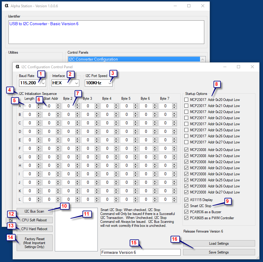
To better understand each of the elements shown in the screenshot, a summary of functions will be indicated below.
- Baud Rate allows you to choose between all available communication data rates supported by this device. The default recommended baud rate is 115.2K Baud, but speeds up to 230,400 are also supported.
- The Interface options determine if values will be shown in Hex (recommended) or decimal values.
- The I2C Port Speed is used to define the communication speed between the serial to i2C converter and the I2C port. The default speed is 100KHz; however, speeds up to 400KHz are also supported, but may cause errors with longer cables. If you intend to use really long I2C cables, the 38KHz speed is also supported.
- This control panel is used to send I2C data to I2C devices when power is first applied. This is useful for initializing I2C chips into a default state, such as displays, relay controllers, PWM controllers, and other devices that may need a few initialization commands to get them working properly.
- Start by entering the length of the I2C communication command.
- Enter the start address of the device you would like to initialize.
- Fill in data bytes for initialization parameters.
- The Startup Options shown here are used to configure common chips for relay control applications. Display configuration is also supported. This control panel serves as a shortcut to the more complicated byte-level initialization.
- Smart I2C Stop will send a I2C Stop Command only when a I2C device communication transaction is successful. Disabling this feature will send a I2C Stop Command Regardless of success or failure. Turning this option off will cause problems with the I2C Bus Scan feature.
- The I2C Bus Scan features searches the I2C port and lists all detected I2C Start Addresses in the display window 11.
- Displays Lists of I2C Start Addresses when the I2C Bus Scan is clicked.
- CPU Soft Reboot simply restarts the firmware in the Serial to I2C Converter.
- CPU Hard Reboot crashes the Serial to I2C Converter forcing the internal Watchdog Timer to reboot the CPU.
- Sets a few important parameters back to factor default values and saves them to the I2C converter.
- Displays the firmware version.
- Load and Save Device Settings. Be sure to Save your settings if any changes are made to this control panel.